Often there is the need to control the power state of a module (sub-circuit). That is, you want to turn on or off the power (= current) that flows to a group of components inside the circuit.
Powering An Isolated Module
If the module is isolated from the rest and allowed to have its own ground voltage level then you can simply control the current flowing out of the module with a switch transistor placed where the module would otherwise connect to common ground. The ground voltage level of the module is then offset against the rest of the circuit by the Collector-Emitter (for NPN bipolar transistors) or Drain-Source (for N-channel FETs) voltage.
Common Ground
You can use a switch transistor in combination with a PNP bipolar transistor or P-channel FET to control the current flow into the module from the supply voltage end. This preserves the common ground voltage level in the module, which is important if the module has connections to other modules in the circuit. If your supply voltage is not much higher than the voltage you want to feed into the module you may have to use a PNP BJT because VEB,sat will be lower than VSG,th on the PMOS.
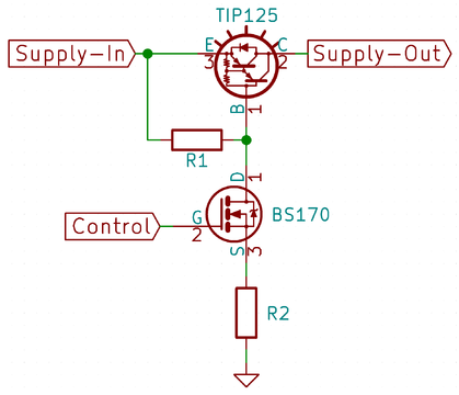
Here is an example power gate circuit consisting of a TIP125 PNP Darlington transistor and BS170 N-channel field effect transistor.

When Control is low (0 V), the channel between the Source and Drain pins of the BS170 is closed. Only little current flows through R1, and VD is close to the supply voltage. VEB of the TIP125 is therefore low and no current can flow from its Emitter pin to its Collector pin. When Control is high (3.3 or 5 V), the channel between Source and Drain of the BS170 becomes conductive and pulls VD down, which in turn increases VEB such that the TIP125 starts conducting current between Emitter and Collector. The value of R2 affects the current flowing to the Base of the TIP125 and, therefore, the maximum current that passes from its Emitter pin to its Collector pin.
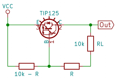
Thanks to the steep switching characteristics of the TIP125 this combination works rather well. The following experimental setup was realized with a potentiometer connected to Base.

| R (kΩ) | 9.26 | 9.12 | 9.0 | 8.9 | 8.8 | 8.73 | 8.67 | 8.6 | 8.53 | 8.46 | 6.28 | 5.11 | 3.7 | 1.9 | 0.3 |
| Vout | 0.01 | 0.22 | 1.3 | 2.3 | 3.5 | 4.7 | 5.7 | 6.7 | 7.7 | 7.9 | 7.95 | 7.94 | 7.9 | 7.8 | 7.6 |
| R | IR | I10k - R | VB | VC |
|---|---|---|---|---|
| 10 kΩ | 0.82 mA | 0.81 mA | 8.2 V | 0 V |
| 300 Ω | 19.5 mA | 0.21 mA | 6.8 V | 7.5 V |