Nucleo-32: Difference between revisions
| (7 intermediate revisions by the same user not shown) | |||
| Line 9: | Line 9: | ||
<br /> | <br /> | ||
==== Pin Layout ==== | ==== Pin Layout ==== | ||
Nucleo-32 boards | The pin layout of Nucleo-32 boards is compatible with [https://store.arduino.cc/products/arduino-nano Arduino Nano] and the STM32 pin names are mostly identical. | ||
[[File:Nucleo-STM32F042-pins.png | x320px | alt="Nucleo-32 STM32F042 pins" ]] | [[File:Nucleo-STM32F042-pins.png | x320px | alt="Nucleo-32 STM32F042 pins" ]] | ||
| Line 45: | Line 45: | ||
<br /> | <br /> | ||
<br /> | <br /> | ||
==== Clock speed ==== | ==== Clock speed ==== | ||
The value for the high-speed external clock (HSE) speed is set by the ''HSE_VALUE'' preprocessor definition. The default value is 8 MHz. You shouldn't need to change this. The clock speed multiplier for is given by ''RCC_CFGR_PLLMULL'' (RCC = Reset and Clock Control, PLL = Phase Locked Loop). When setting up a new project, GNU MCU Eclipse Plugin pops up a dialog where CPU parameters such as Flash memory size, RAM size, and clock speed can be specified. The given value for the clock speed is then placed into the compiler command line argument -DHSE_VALUE. | The value for the high-speed external clock (HSE) speed is set by the ''HSE_VALUE'' preprocessor definition. The default value is 8 MHz. You shouldn't need to change this. The clock speed multiplier for is given by ''RCC_CFGR_PLLMULL'' (RCC = Reset and Clock Control, PLL = Phase Locked Loop). When setting up a new project, GNU MCU Eclipse Plugin pops up a dialog where CPU parameters such as Flash memory size, RAM size, and clock speed can be specified. The given value for the clock speed is then placed into the compiler command line argument -DHSE_VALUE. | ||
| Line 50: | Line 51: | ||
<br /> | <br /> | ||
=== | ==== Power supply considerations ==== | ||
When powering the Nucleo-32 board with an external 5 V power supply, you need to either open solder bridge 9 or you can connect the ''VIN'' pin to 5 V as well. If the solder bridge remains closed, the ''T_NRST'' pin of the disabled ST-LINK controller will constantly reset the main controller by pulling down the ''NRST'' pin. With 5 V supplied to both ''+5V'' and ''VIN'', the ST-LINK part has enough power to pull up ''T_NRST''. After the development phase, as part of deploying the microcontroller application, SB9 should be opened and the wiring changed to supply power only to ''+5V'' (or ''+3V3'') in order to keep power consumption low. | |||
<br /> | <br /> | ||
<br /> | <br /> | ||
| Line 112: | Line 102: | ||
=== Programming === | === Programming === | ||
The STM32 API is the main programming interface for STM32, for which I recommend using [https://www.st.com/en/development-tools/stm32cubeide.html STM32CubeIDE]. For Mbed-enabled boards, you can use [https://os.mbed.com Mbed OS], which provides higher-level, C++ interfaces. At the lower level, you can use [https://developer.arm.com/tools-and-software/embedded/cmsis Arm CMSIS], Arm Cortex-M assembly and the programming manual for each microcontroller to work directly on the registers that | |||
Reference and Programming Manuals for some STM32 Microcontrollers | |||
* [http://www.st.com/resource/en/programming_manual/dm00051352.pdf STM32F0xxx Programming Manual] | |||
* [https://www.st.com/resource/en/reference_manual/rm0091-stm32f0x1stm32f0x2stm32f0x8-advanced-armbased-32bit-mcus-stmicroelectronics.pdf STM32F0xx Reference Manual] | |||
* [https://www.st.com/resource/en/programming_manual/pm0214-stm32-cortexm4-mcus-and-mpus-programming-manual-stmicroelectronics.pdf STM32 Cortex-M4 Programming Manual] | |||
* [https://www.st.com/resource/en/reference_manual/rm0394-stm32l41xxx42xxx43xxx44xxx45xxx46xxx-advanced-armbased-32bit-mcus-stmicroelectronics.pdf STM32L4xxxx Reference Manual] | |||
* [https://www.st.com/resource/en/reference_manual/rm0316-stm32f303xbcde-stm32f303x68-stm32f328x8-stm32f358xc-stm32f398xe-advanced-armbased-mcus-stmicroelectronics.pdf STM32F3xxx Reference Manual] | |||
* | |||
<br /> | <br /> | ||
<br /> | <br /> | ||
| Line 245: | Line 243: | ||
Please refer to section 4.4 of the [http://infocenter.arm.com/help/index.jsp?topic=/com.arm.doc.dui0497a/index.html ARM Cortex-M0 Devices Generic User Guide] to learn more about SysTick and how it is used. | Please refer to section 4.4 of the [http://infocenter.arm.com/help/index.jsp?topic=/com.arm.doc.dui0497a/index.html ARM Cortex-M0 Devices Generic User Guide] to learn more about SysTick and how it is used. | ||
<br /> | <br /> | ||
<br /> | <br /> | ||
Latest revision as of 2022-09-18T16:08:21
Introduction
The Nucleo-32 STM32F042 development board features the ARM Cortex-M0 based STM32F042K6 microcontroller with 48 MHz clock speed, 32 KB Flash storage and 6 KB static RAM.
Hardware
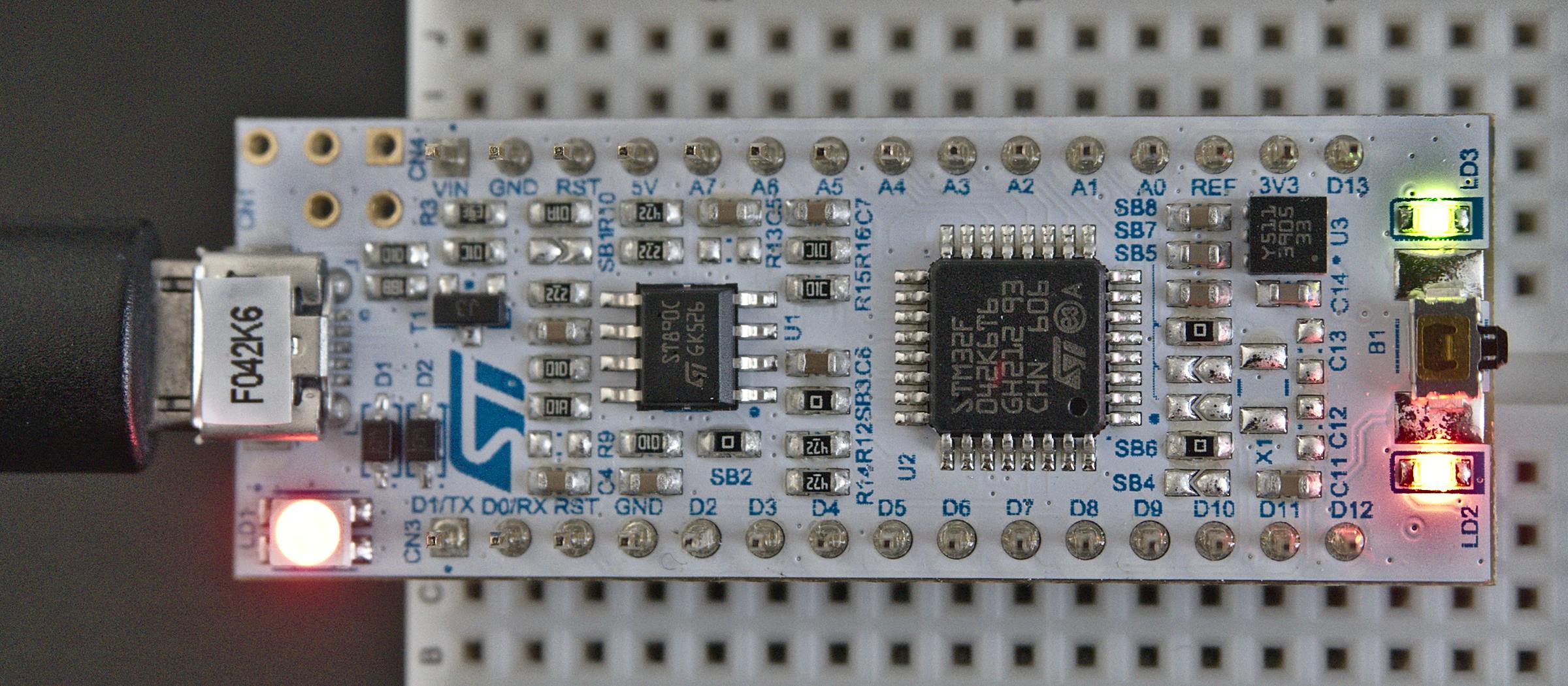
The hardware is described in the STM32 Nucleo-32 board user manual, which applies to all Nucleo-32 boards. The board is sized like an Arduino Micro, 20 pins tall (one-tenth-inch pin spacing) and 7 pins wide. The pins on the board are compatible with the Arduino Nano so that the same extension boards can be attached.
Pin Layout
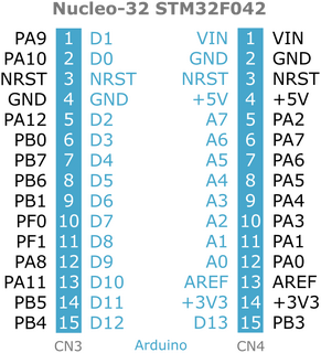
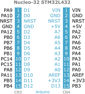
The pin layout of Nucleo-32 boards is compatible with Arduino Nano and the STM32 pin names are mostly identical.
Solder Bridges
There are a number of solder bridges on both sides of a Nucleo-32 board. They are labeled with the SB prefix. Solder bridges are used for (permanently) reconfiguring the board. They are cheaper than, for example, DIP switches and take little space on circuit boards. Some solder bridges on the Nucleo have solder on both ends and an air gap in between. These are in OFF state. The two ends need to be short-circuited with solder to switch them to the ON state. Other solder bridges have a resistor between the soldered ends. These bridges are in ON state. The resistor needs to be desoldered to switch them to the OFF state. Some of the solder bridges that are ON by default are explained in the table below.
| Bridge | Description |
|---|---|
| SB9 | Connects the NRST reset signal from ST-LINK to the NRST pin of STM32. Disconnect when using an external power supply. |
| SB10 | Connects VREF+ to VDD by default. Otherwise VREF+ is provided by pin 13 on header row CN4. |
| SB11 | Connects VSS to pin 16 of the STM32 (U2). Disconnecting frees up pin 16 on Nucleo STM32F031 boards for use as GPIO pin PB2. |
| SB13 | Connects VSS to pin 32 of the STM32. Disconnecting frees up pin 32 on Nucleo STM32F031 boards for use as GPIO pin PB8. |
| SB12 | Connects pin 31 of the STM32 to Ground via a 10 kΩ pull-down resistor so that pin 31 is used as BOOT0 pin. Disconnecting frees pin 31 on Nucleo STM32F042 boards for use as GPIO pin PB8. |
| SB15 | Connects the green LED LD3 to the Arduino pin D13. |
| SB16 | Connects pin 7 on header row CN4 to STM32 pin PB6 so that Arduino Nano pin A5 can be used as I2C SDA. Disconnecting makes pin 7 usable as Arduino Nano analog input A5 while breaking I2C capability. |
| SB18 | Connects pin 8 on header row CN4 to STM32 pin PB7 so that Arduino Nano pin A4 can be used as I2C SCL. Disconnecting makes pin 8 usable as Arduino Nano analog input A4 while breaking I2C capability. |
SB2 and SB3 are for disconnecting the USART interface from ST-LINK/V2-1 with which the STM32 is can be flashed and debugged via USB.
Clock speed
The value for the high-speed external clock (HSE) speed is set by the HSE_VALUE preprocessor definition. The default value is 8 MHz. You shouldn't need to change this. The clock speed multiplier for is given by RCC_CFGR_PLLMULL (RCC = Reset and Clock Control, PLL = Phase Locked Loop). When setting up a new project, GNU MCU Eclipse Plugin pops up a dialog where CPU parameters such as Flash memory size, RAM size, and clock speed can be specified. The given value for the clock speed is then placed into the compiler command line argument -DHSE_VALUE.
Power supply considerations
When powering the Nucleo-32 board with an external 5 V power supply, you need to either open solder bridge 9 or you can connect the VIN pin to 5 V as well. If the solder bridge remains closed, the T_NRST pin of the disabled ST-LINK controller will constantly reset the main controller by pulling down the NRST pin. With 5 V supplied to both +5V and VIN, the ST-LINK part has enough power to pull up T_NRST. After the development phase, as part of deploying the microcontroller application, SB9 should be opened and the wiring changed to supply power only to +5V (or +3V3) in order to keep power consumption low.
Bootloader
STM32 microcontrollers come with a built-in bootloader on an integrated ROM. Depending on the logical value of the BOOT0 hardware pin or the value of the BOOT0 option byte (OB - stored in a special region in flash memory), the bootloader is executed instead of the user program in flash memory. The bootloader thus runs after the system has been initialized as usual (plus I2C and USB Full Speed drivers). The bootloader will check for data on the USART, I2C and USB serial communication lines, in that order, and run the appropriate subroutine for storing the incoming data in the user program region of the flash memory.
On STM32F042, the bootloader is activated by one of these combinations
- Boot0 (hardware pin) = 1 and nBoot1(bit) = 1 and nBoot0_SW(bit) = 1
- nBoot0 (software bit) = 0 and nBoot1(bit) = 1 and nBoot0_SW(bit) = 0
- Boot0 (hardware pin) = 0 and nBoot0_SW (software bit) = 1 and main flash memory is empty
The BOOT0 hardware pin is pin 31 of the STM32. By default, it is connected to Ground via a pull-down resistor and a solder bridge that can be desoldered for changing the configuration permanently.
Refer to chapter 7 of the application note AN2606 for the specific of the STM32F04xxx bootloader.
OpenOCD and the USART Bootloader
Some STM32 experimentation boards are designed so that the user can select the boot mode with a jumper. The Nucleo STM32F042 does not expose the BOOT0 pin with a header. Furthermore, OpenOCD does not require a physical change on the board in order to flash the user program. So, how does this software-only method of activating the bootloader work?
Using the DFU Bootloader
DFU (Device Firmware Update) is part of the USB standard and specifies the process of sending (firmware) code to a USB-connected device.
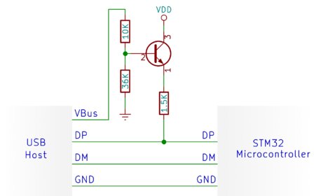
The schematic below shows how an external pull-up resistor can be connected to USB_DP if needed. 
STM32F04 configuration for DFU system memory boot mode (from AN2606)
| Feature/Peripheral | State | Comment |
|---|---|---|
| USB | Enabled | USB used in FS mode |
| USB_DM line | Input/Output | Connect to pin PA11 on STM32. |
| USB_DP line | Input/Output | Connect to pin PA12 on STM32. No external pull-up resistor required. |
Interestingly, connecting the USB cable to a USB power outlet prevents the Nucleo from booting into the flashed user program.
Programming
The STM32 API is the main programming interface for STM32, for which I recommend using STM32CubeIDE. For Mbed-enabled boards, you can use Mbed OS, which provides higher-level, C++ interfaces. At the lower level, you can use Arm CMSIS, Arm Cortex-M assembly and the programming manual for each microcontroller to work directly on the registers that
Reference and Programming Manuals for some STM32 Microcontrollers
- STM32F0xxx Programming Manual
- STM32F0xx Reference Manual
- STM32 Cortex-M4 Programming Manual
- STM32L4xxxx Reference Manual
- STM32F3xxx Reference Manual
Memory Model
| Start | End | Size | Label | Access Type | Description |
|---|---|---|---|---|---|
| 0x00000000 | 0x1FFFFFFF | 512 MB | Code | Normal | Region for executable code and data. |
| 0x20000000 | 0x3FFFFFFF | 512 MB | SRAM | Normal | Region for executable code and data. |
| 0x40000000 | 0x5FFFFFFF | 512 MB | Peripheral | Device | external |
| 0x60000000 | 0x9FFFFFFF | 1 GB | External RAM | Normal | Data-only region |
| 0xA0000000 | 0xDFFFFFFF | 1 GB | External Device | Device | external |
| 0xE0000000 | 0xE00FFFFF | 1 MB | Private Peripheral Bus | Strongly Ordered | Reserved for core peripheral registers (NVIC, system timer, system control block). Access performed word by word. |
| 0xE010.0000 | 0xFFFFFFFF | 511 MB | Device | Device | Includes all the STM32 standard peripherals. |
| Type | Description |
|---|---|
| Normal | The sequence of access can be changed by the processor in order to predictively minimize wait times. |
| Device | The sequence is preserved relative to other memory accesses of this type or of the Strongly Ordered type. |
| Strongly Ordered | The sequence is preserved relative to all other memory accesses |
STM32F042 addresses of interest
- On reset, the main stack pointer (MSP) points at 0x200017e8 in SRAM.
- Option Bytes start at 0x1FFFF800
- GPIO ports (only A, B, and F available)
- A starts at 0x48000000
- B starts at 0x48000400
- F starts at 0x48001400
- SysTick base address is 0xE000E010
- NVIC base address is 0xE000E100
- System Control Block (SCB) base address is 0xE000ED00
Memory Barrier Instructions
In order to optimize performance, the processor may fetch memory contents ahead of execution of a memory access instruction while a previous instruction is being executed. Memory barrier instructions should be used if the program logic depends on the sequence of memory access. These are
DMB             ; Data Memory Barrier
DSB             ; Data Synchronization Barrier
ISB             ; Instruction Synchronisation Barrier
GPIO
Control Registers
The GPIO port control registers are accessed through memory locations that connect to the Advanced High-performance Bus (AHB) of the Cortex-M0 processor. Each GPIO port is controlled by the registers listed below. In each register, the setting for an individual pin of a GPIO port is stored in certain bits inside the register. Since each port has up to 16 pins and registers are at most 32 bits wide, the setting for each pin can be up to 2 bits wide.
| register name | length (bytes) | offset (bytes) | description |
|---|---|---|---|
| MODER | 4 | 0x00 | mode register, 2 bits per pin, modes: In (0x00), Out (0x01), Alternate Function (0x02), Analog In/Out (0x03) |
| OTYPER | 2 | 0x04 | output type register, 1 bit per pin, two types defined: PP (0x00), OD (0x01) |
| RESERVED0 | 2 | 0x06 | reserved |
| OSPEEDR | 4 | 0x08 | output speed register, 2 bits per pin, three speeds defined: Level1 (0x00), Level2 (0x01), Level3 (0x03) |
| PUPDR | 4 | 0x0C | pull-up/pull-down register, 2 bits per pin, three modes defined: NoPull (0x00), Up (0x01), Down (0x02) |
| IDR | 2 | 0x10 | input data register, 1 bit per pin, two modes defined: |
| RESERVED1 | 2 | 0x12 | reserved |
| ODR | 2 | 0x14 | output data register, 1 bit per pin, two modes defined: |
| RESERVED2 | 2 | 0x16 | reserved |
| BSRR | 4 | 0x18 | bit set/reset register, 2 bits per pin, 1 bit for set in the lower half word, 1 bit for reset in the upper half word |
| LCKR | 4 | 0x1C | configuration lock register, 1 bit per pin within the lower half word, upper half word for locking the complete port |
| AFRL | 4 | 0x20 | alternate function register for pins 0 through 7, 4 bits per pin |
| AFRH | 4 | 0x24 | alternate function register for pins 8 through 15, 4 bits per pin |
| BRR | 2 | 0x28 | bit reset register, 1 bit per pin, two modes defined: |
| RESERVED3 | 2 | 0x2A | reserved |
Available GPIO Pins
The Nucleo-32 STM32F042 board comes with GPIO header pins for ports A (registers' base address: 0x48000000), B (registers' base address: 0x48000400) and F (registers' base address: 0x48001400). Specifically, the pins are A0–A12, B0, B1, B3–B7, F0, and F1.
Initialization
System Timer (SysTick)
Control Registers
SysTick, the 24-bit system timer, is controlled and accessed through four consecutive 32-bit memory locations (starting at 0xE000E010) that connect to the registers of the timer over the Private Peripheral Bus.
| Address | Name | Access Type | Description |
|---|---|---|---|
| 0xE000E010 | CTRL (SYST_CSR) | read/write | Control and status |
| 0xE000E014 | LOAD (SYST_RVR) | read/write | Reload value |
| 0xE000E018 | VAL (SYST_CVR) | read/write | Current value |
| 0xE000E01C | CALIB (SYST_CALIB) | read-only | Calibration |
Usage
Please refer to section 4.4 of the ARM Cortex-M0 Devices Generic User Guide to learn more about SysTick and how it is used.


